
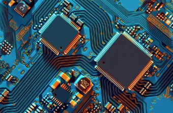
In semiconductor manufacturing, dry-etch chambers using aggressive plasma gases like fluorine and chlorine demand extremely robust and clean materials. Plasma-facing components inside etch chambers, ESCs, and CVD liners face several critical challenges:
- Erosion & Corrosion Resistance : Plasma etching environments rapidly degrade exposed surfaces. Any material loss can result in wafer contamination or unplanned downtime.
- Ultra-High Purity & Particle Cleanliness : Even microscopic contamination can compromise yield. Materials must offer exceptional purity and controlled trace elements to avoid micro-particle release and spalling during wafer processing.
- Thermal & Structural Stability : Coatings must remain phase-stable and inert under high temperatures and prolonged plasma exposure, avoiding decomposition or reactions with other materials.
- Dielectric Performance : For components like electrostatic chucks (ESCs), coatings must act as reliable insulators with consistent dielectric properties and mechanical integrity.
OUR SOLUTION : PROPLASMA® HP6.5 TECHNOLOGY
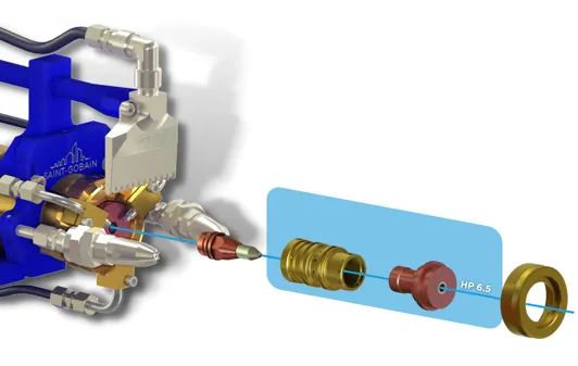
To ensure optimal deposition of our high-purity yttria powders, we recommend the Proplasma® HP6.5 torch configuration. This equipment is specifically suited for precision coatings required in semiconductor environments, such as dry-etch chambers and electrostatic chucks (ESCs).
Proplasma® HP6.5 offers:
- Fine spray control for ultra-smooth, dense coatings with low porosity
- Low energy consumption, enabling efficient deposition of high-cost materials like Y₂O₃
- Superior coating consistency across batches, critical for repeatable process outcomes
- Compact, modular setup ideal for R&D and fab-scale production.
Whether you're coating small components or complex geometries, Proplasma® HP6.5 ensures reliable, repeatable results with minimal material waste and maximum coating performance.
→ Learn more about our plasma spray equipment here
For semiconductor applications, the HP6.5 configuration is particularly well-suited, offering fine control and high-purity coating consistency, even for the most demanding plasma-facing components.
Interested in testing Proplasma® HP6.5 for your semiconductor application?
OUR SOLUTION : YTTRIA-BASED THERMAL SPRAY POWDERS
At Saint-Gobain Coating Solutions, we offer high-purity Y₂O₃ (yttria) powders engineered for semiconductor applications where purity and plasma resistance are non-negotiable.
Our yttria powders enable:
- Exceptional chemical resistance to aggressive fluorinated and chlorinated plasma chemistries
- Ultra-smooth, dense coatings with minimal porosity for gas-tight protection
- Outstanding dielectric behavior and thermal stability
- Superior consistency and reliability with traceability and “Copy Exact” quality protocols
#1341 High Purity Yttria Powder
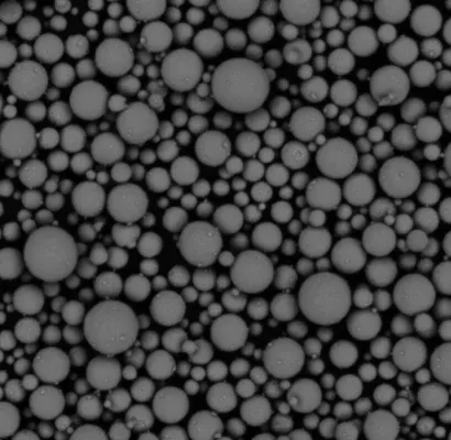
Designed for critical plasma-facing components in dry-etch chambers, ESCs, CVD liners.
Key features:
- Densified spherical morphology for highly uniform, dense coatings
- Ultra-narrow particle size distribution (10–30 µm) for fine spray control and mechanical cohesion
- Coating porosity < 1% achievable, enabling gas-tight protection
- Purity > 99.995% Y₂O₃, ideal for ultra-clean semiconductor environments
- Exceptional plasma resistance over extended exposure cycles
- Certified consistency and traceability, backed by 20+ years of industrial validation
#1341 is a game changer for achieving denser, purer, and more consistent coatings. When combined with our Proplasma® HP6.5 torch, it delivers:
- Powder feed rates up to 70 g/min
- Deposit efficiency exceeding 60%
- Enhanced coating quality and improved process productivity
Our powders are optimized for thermal spray processes and come as dense spherical agglomerates, ensuring excellent flowability, high deposition efficiency, and low porosity coatings. In addition to the standard offering, we also offer co-development opportunities to tailor custom formulations for specific semiconductor process needs.
Need a sample for qualification?
TYPICAL APPLICATIONS IN SEMICONDUCTOR
- Dry-Etch Chamber Liners & Shields : Superior protection against chemical erosion from aggressive plasma gases
- Electrostatic Chucks (ESCs) : Dielectric insulation with excellent mechanical integrity
- CVD & PVD Liners : Gas-tight coatings that resist degradation under repeated thermal cycles
- Setter Plates & Molten Metal Environments : Chemically inert coatings suitable for advanced sintering and contact with reactive metals
WHY CHOOSE SAINT-GOBAIN COATING SOLUTIONS?
- Ultra-High Purity Expertise : We maintain tight control over morphology and chemistry to deliver consistent, clean coatings every time.
- Field-Tested Reliability : Trusted by fabs and OEMs globally, our yttria powders follow the “Copy Exact” model with full traceability and over two decades of industrial validation.
- Global Reach, Local Support : Our teams around the world provide responsive technical assistance, ensuring the best solution for your process, anywhere
WANT TO LEARN MORE ABOUT YTTRIA #1341?
Access detailed specifications, morphology, and performance data in our Technical Datasheet.

